
From large outdoor billboards to ultrafine pitch indoor LED displays, the packaging technology determines the reliability, specific uses, and quality of the screen.
With suitable LED display packaging technology, you can transform semiconductors with microscopic-sized chips into robust, visual, bright, and accurately aligned communication systems.
In this article, we will explore popular packaging technologies in the LED display industry.
Understanding Packaging in LED Display
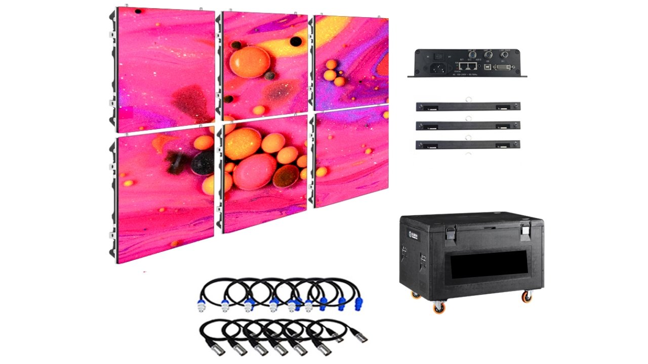
In the LED display manufacturing industry, the term packaging mostly refers to how miniature LED chips are interconnected and protected to form pixels and images.
During packaging, you will use different technologies of chip-level encapsulation and mounting to protect LED chips. By doing so, you connect critical LED components and modules to make screens for use in real-world applications.
Role of Packaging in LED Display Assembly

· Mechanical Protection
The packaging protects sensitive LED chips against moisture and dust, vibration, and mechanical stress during manufacturing, installation, and long-term exposure to the external environment.
· Electrical Interconnection
Through packaging, you achieve electrical connections between LED chips and circuit boards to guarantee stable transmission of each signal and predictable pixel activation.
· Heat Dissipation
Good packaging materials and designs direct the heat out of the LED junctions, avoiding thermal degradation and early brightness decay.
· Optical Performance Control
The entire aspect of packaging can affect light transmission efficiency, color uniformity, and viewing angle using lens shaping and encapsulation material choice.
· Pixel Pitch Definition
The density of the pixels and the viewing distance achievable are directly controlled by the packaging. Therefore, it defines the closeness of the LED pixels, thereby defining the resolution and density of the pixels.
· Structural Integration
With packaging, LED chips can be delivered as standardized modules, making it easier to scale, have strategies of repair, as well as integrating modules at the system level.
· Environmental Protection
Packaging improves protection against humidity, ultraviolet radiation, oxidation, and corrosion in indoor, outdoor, and high-brightness conditions.
Evolution of LED Display Packaging Methods

Over the years, there has been significant evolution in the LED display packaging industry. As a matter of fact, you have certainly come across phrases like DIP, COB, or SMD. All these refer to unique technologies in LED screen assembly to meet specific performance requirements.
Let’s explore each of these packaging technologies:
1. Dual In-line Packaging (DIP)
DIP packaging connects the separate chips of red, green, and blue LEDs into the lamp housings made of epoxy with protruding electrical leads. One lamp is inserted through the circuit boards individually or semi-automatically and soldered into visible pixel clusters.
Benefits
DIP has high brightness, high heat, and the best outdoor visibility in conditions of direct sunlight.
Limitations
Unfortunately, DIP has a big physical size, limited pixels, and resolution. These are some of the reasons why you will not find DIP LED display packaging in compact electronics.
Applications
The use of DIP is still popular in large-sized billboards, stadium terminals, and highway signs that require maximum brightness and longer service lifespan.
2. Surface-Mounted Device Packaging (SMD)
SMD is the combination of red, green, and blue LED chips, which are mounted on one compact unit soldered onto PCB surfaces. By using automated pick-and-place machines, you can achieve high consistency in manufacturing with accuracy in alignment.
Benefits
With SMD, you can achieve a small pixel pitch, expanded viewing angles, smooth color mixing, and higher resolution display construction.
Limitations
The bare LED platforms are susceptible to moisture, impact, and surface contamination without protective layers over them.
Applications
SMD is popular in indoor applications, rental LED screens, control rooms, retail signage, and broadcast studio settings.
3. Glue on Board Packaging (GOB)
GOB uses the clear coat of epoxy or silicone directly on mounted SMD LEDs and covers the whole module. This is an advanced LED packaging technology known for higher protection and enhanced durability.
Benefits
Such encapsulation is much better in enhancing impact resistance, moisture protection, and surface durability without causing changes in pixel arrangement.
Limitations
The improper formulation of the material may result in yellowing, bubbles, or optical degradation when subjected to long-term heat and ultraviolet radiation.
Applications
You can use GOB in interior high-traffic installations, rental displays, and interactive environments that need to be handled and cleaned frequently.
4. Chip on Board Packaging (COB)
For COB packaging, you will mount LED chips on ceramic or PCB. You will then seal them with epoxy, which creates a compact and efficient lighting source.
Furthermore, this LED packaging technology is known to offer improved brightness, which is better than the SMD LEDS
Benefits
COB LED has ultra-small pixel pitch, enhanced heat dissipation, smooth surfaces, and high contrast operation.
Limitations
Simple repair of individual pixels proves difficult, and in most cases, it might need the replacement of modules instead of mere reworking of components.
Applications
COB finds significant applications in the high-resolution indoor displays, control centers, boardrooms, and high-end visualization areas.
5. Mini LED in Package (MiP)
MiP produces Mini LED chips, which are pre-packaged as tiny surface mount packages and then assembled on a circuit board. It is a perfect choice when you are looking for Mini/Micro LED displays.
Remember, this LED packaging solution was invented to bridge the gap between COB and SMD.
Benefits
MiP is a combination of high pixel control, better yield rates, and higher reparability than direct chip mounting. You can also achieve ultra-fine pixels as low as below P0.7.
Limitations
The complexity in manufacturing and the cost are currently barriers to large-area commercial displays being widely adopted.
Applications
You can use MiP for fine-pitch high-end displays, television broadcast studios, and new premium indoor high-image markets.
6. Integrated Matrix Devices in LED Packaging
IMDs combine arrays of LEDs, i.e., several LEDs, in unified arrays that are pre-aligned and linked electrically in single packages.
Benefits
They enhance assembly speed, pixel consistency, and scalability of production, especially in complicated display structures.
Limitations
It has less design flexibility and fewer customization options than discrete packaging approaches.
Applications
They are applied in customized business exhibitions, auto visualization, and industrial LED matrix.
7. Chip on Film in LED Packaging (COF)
COF places the LED chips on its flexible film substrates, and this allows for ultra-thin, bendable configurations of the display modules. It is a flexible packaging technology allowing you to make many innovative LED display solutions.
Benefits
COF accommodates lightweight designs, curved surfaces, and installations that are space-constrained with lower structural thickness.
Limitations
Limited outdoor life and mechanical frailty limit the ability to use the product in harsh operating conditions.
Applications
You can use this LED display packaging technology in creative performance, architectural installations, wearable displays, and experimental formats of visualization.
Technical Comparison of Different LED Display Packaging

| Type of LED Packaging Technology | Pixel Pitch | Viewing Angle | Brightness | Durability |
| DIP | High pixel pitch but sacrifices resolution. | The angles are moderate because of the discrete lamp structures. | Provides an even greater brightness. | High outdoor durability. |
| COB | COB allows a very fine pixel pitch. | High thermal control and high viewing angles. | Ultra-high brightness. | This is because of built-in encapsulations that enhance durability. |
| SMD | SMD helps in small pixel pitch. | Un-grain color mixing and expansive viewing range. | High brightness. | Environmental protection measures are crucial in determining the durability. |
| MiP | MIP Attains extremely low pixel pitch | Angular clarity is also good with sophisticated optical constructions. | Enhanced repairability as well as brightness control. | MIP has excellent moisture and dust resistance, hence more durable than SMB and COB. |
| GOB | GOB Maintains SMD pixel pitch | The angle of view does not change, although optical clarity is determined by the quality of encapsulation. | GOB has a high brightness similar to that of SMD | GOB shows a vast improvement in the durability of the surface. |
Factors to Consider when Choosing LED Display Packaging

- Thermal management: The brightness stability, lifespan, and color stability during continuous operation are determined by thermal management.
- Pixel pitch: The choice of pixel pitch is based on the viewing distance, resolution, and the constraints of the installation space.
- LED display applications: Applications in LED displays determine brightness, durability, and maintenance requirements in indoor, outdoor, or rental applications.
- LED display reliability: The reliability of LED displays is based on the resistance to moisture, heat cycling, mechanical stress, and ultraviolet exposure of packaging.
- Manufacturing complexity: The complexity of manufacturing has implications for yield rates, repair plans, scalability, and the control of production costs in the long run.
- Cost: The element of costs balances the initial investment with the lifespan of operation, frequency of maintenance, and appearance expectations.
- Brightness requirements: Brightness needs determine packaging, optical design, power design, and thermal design margin.
FAQs

Does LED display packaging affect the pixel pitch and density?
Yes, packaging is what determines the spacing between the LEDs that can be mounted, the pixel pitch, and the display resolution.
How des LED display affect the viewing angle and brightness?
Optical output is determined by packaging and affects the dispersion of light, color mixing, brightness performance, and useful viewing angles.
Is MIP better than COB for small pixel pitch?
MIP is preferable in terms of repairability and yield, but COB has a slightly superior thermal performance at very small pixel spaces.
Can you repair the LED display packaging if the pixels are faulty?
Repairability is easier in SMD and MiP and is more common at a module level in COB.
Why do GOB packaging turn yellow or bubble after some time?
Poor-quality encapsulation materials fail when subjected to heat and UV rays, thus turning color or trapping gas.
Which LED packaging has the lowest Moiré effect for filming?
COB is LED packaging that results in smooth surfaces and even light output, which substantially decreases Moiré patterns when filming.
Partner with JYLED for all LED Displays

JYLED is a trusted LED display manufacturer in China. For over 10 years, we have been making different LED displays that are custom-made to match our clients’ unique requirements and specifications.
You can choose from our pole LED display, LED billboard trailer, curved LED screen, matrix LED screen, or any unique option that matches your project. At JYLED, we have a unique LED display for any application – request our product catalogue now.

